Glass substrates are getting fresh attention in the semiconductor industry. On July 24, 2026, Intel and Lens Technology announced a collaboration to explore glass substrate-based packaging for future AI and data-center systems. The term describes a layer inside a chip package, not the silicon chip itself.
What Is a Glass Substrate?
A substrate is the foundation that supports one or more silicon dies and routes electrical connections between those dies and the circuit board. Most package substrates use organic materials. A glass substrate, also known as a glass-core substrate, replaces part of that foundation with specially engineered glass.
That matters because modern processors increasingly place several smaller dies, called chiplets, inside a single package. A CPU, graphics processor and high-bandwidth memory may require huge numbers of closely packed connections. As a result, the package has become almost as important as the chips it contains.
How Does It Work?
The glass doesn’t carry the chip’s electrical signals. Instead, engineers build metal wiring layers on and around it, then form tiny vertical openings called through-glass vias that carry connections through the glass. Silicon dies sit above the substrate, while contacts underneath connect the completed package to a circuit board.
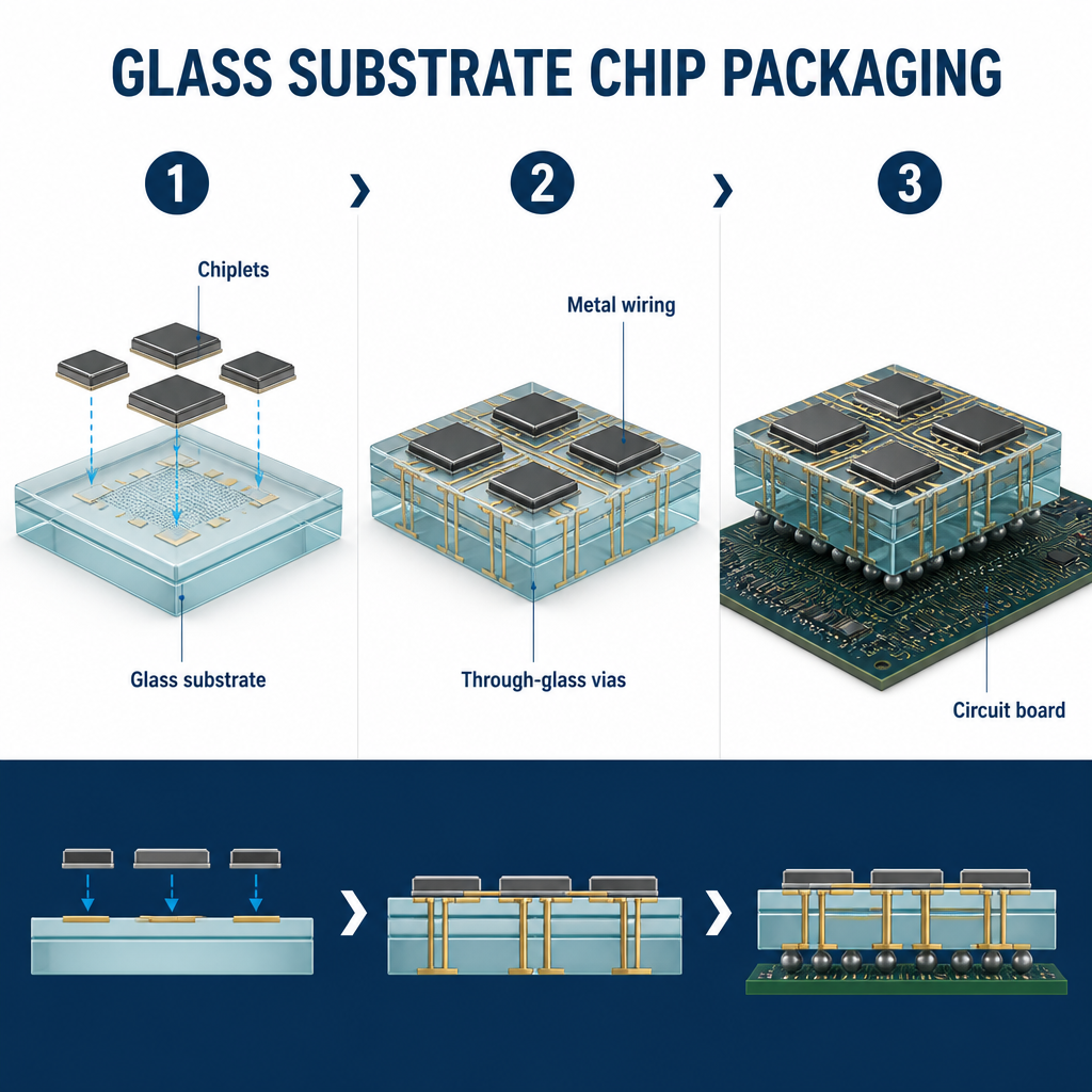
Compared with conventional organic substrates, glass can offer a flatter, more dimensionally stable base. This may help manufacturers produce finer wiring patterns as well as larger, denser packages. It could also help designers handle the signal and power-delivery demands that arise when many chiplets communicate at high speed.
Why Does It Matter?
AI servers and high-performance computers need more compute, memory bandwidth and electrical connections than traditional single-chip designs can easily deliver. Glass substrates offer one possible way to scale advanced packaging without making a single silicon die larger.
The technology is still emerging and isn’t yet a standard feature in everyday processors. Producing glass with precise holes, metal layers and reliable connections remains difficult. But as chipmakers pursue larger multi-chip packages for AI, cloud and specialized computing, glass substrates have become an important material to watch.